logo
オンラインです

Thin-Film Technology

Thin-Film Technology

大画像 :  Thin-Film Technology

商品の詳細:
起源の場所: 中国
ブランド名: ZG
証明: CE
モデル番号: MS
お支払配送条件:
最小注文数量: 1個
価格: 10USD/PC
パッケージの詳細: 世界中に発送できる丈夫な木箱
受渡し時間: 5~8営業日
支払条件: L/C、D/A、D/P、T/T、ウェスタンユニオン、マネーグラム
供給の能力: 1000個

Thin-Film Technology

説明
ハイライト:

thin-film ceramic components

,

technical ceramic thin-film parts

,

thin-film technology ceramic materials

Thin-Film Technology

The manufacture of boards using thin-film technology has today become very widespread in the production of micro- and nanoelectronics.


With thin-film technology, an adhesive and basic functional layer is deposited on the ceramic base. Deposition of layers can be performed by PVD (Physical Vapor Deposition), CVD (Chemical Vapor Deposition) or ALD (Atomic Layer Deposition) methods. The most commonly used PVD methods of deposition of thin films, as the easiest to implement and productive.


After the deposition of the main functional layer, if its thickness is not sufficient for the final product, its galvanic build-up of the material is carried out.


To form a topology pattern with further chemical etching, a lithography process is carried out. Chemical etching of the conductive and adhesive layer is carried out in special etchants.


The last stage is the application of a finishing coating to protect the metallization surface from oxidation, preserving the solderability of giving the finished product a marketable appearance.


Thin-Film Technology 0


The technological process steps:

1. Formation of a film of the required material on a ceramic substrate (the coating can be single-layer or multi-layer). Most often, a two-layer coating is formed - a thin film of the adhesive sublayer and a film of the main functional layer;


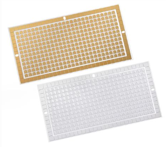
2. Applying photoresist to the formed layer;


3. Exposure and manifestation of photoresist;


4. Chemical etching of the deposited main functional coating;


5. Removing the photoresist from the surface of the board;


6. Application of the finishing coating.


Thanks to thin-film technology, it became possible to manufacture thin-film active and passive elements, which made it possible to reduce the dimensions of the final electronics products and increase their performance.


Ceramic AlN (aluminum nitride) and Al2O3 (polycor BK100) are used as substrates;


Conductive materials are used to form the topology. The most commonly used: Cu, Al. Thanks to thin-film technology, it is possible to form optically transparent conductive ITO (In-SnOxide) films.


Active and passive elements are formed from various dielectric and conductive materials.


Metals, metal alloys and organic compounds can be used as finishing materials. The most widely used coatings are chemical nickel-immersion gold, immersion silver, immersion tin, electroplating and others.


Depending on the required accuracy, the conductor-gap distance, the type of resistor and the method of lithography are selected. The most commonly used are photoresists and the photolithography process.


Specifications

Check the characteristics of products sold using thin-film technology with our specialists

Application area

  • power integrated circuits;
  • various micro- and nanoelectronics products;
  • thermoelectric coolers and generators;
  • GIS microwave, etc.

連絡先の詳細
HENAN ZG INDUSTRIAL PRODUCTS CO.,LTD

コンタクトパーソン: Daniel

電話番号: 18003718225

ファックス: 86-0371-6572-0196

私達に直接お問い合わせを送信 (0 / 3000)